It is the process of growing single crystals of semiconductors (e.g. silicon, germanium and gallium arsenide), metals (e.g. palladium, platinum, silver, gold), salts, and synthetic gemstones.
The process is named after Polish scientist Jan Czochralski, who discovered the method in 1916 while investigating the crystallization rates of metals.
 The most important application may be the growth of large cylindrical ingots, or boules, of single crystal silicon. Other semiconductors, such as gallium arsenide, can also be grown by this method, although lower defect densities in this case can be obtained using variants of the Bridgman-Stockbarger technique.
 A large, single-crystal, cylindrical ingot is extracted from the melt by precisely controlling the temperature, rate of pulling and speed of rotation.
Due to the efficiencies of common wafer specifications, the semiconductor industry has used wafers with standardized dimensions. In the early days, the boules were smaller, only a few inches wide. With advanced technology, high-end device manufacturers use 200 mm and 300 mm diameter wafers. The width is controlled by precise control of the temperature, the speeds of rotation and the speed the seed holder is withdrawn. The crystal ingots from which these wafers are sliced can be up to 2 metres in length, weighing several hundred kilograms. Larger wafers allow improvements in manufacturing efficiency, as more chips can be fabricated on each wafer, so there has been a steady drive to increase silicon wafer sizes. The next step up, 450 mm, is currently scheduled for introduction in 2012. Silicon wafers are typically about 0.2–0.75 mm thick, and can be polished to great flatness for making integrated circuits, or textured for making solar cells.
The process begins when the chamber is heated to approximately 1500 degrees Celsius, melting the silicon. When the silicon is fully melted, a small seed crystal mounted on the end of a rotating shaft is slowly lowered until it just dips below the surface of the molten silicon. The shaft rotates counterclockwise and the crucible rotates clockwise. The rotating rod is then drawn upwards very slowly, allowing a roughly cylindrical boule to be formed. The boule can be from one to two metres, depending on the amount of silicon in the crucible.
The electrical characteristics of the silicon are controlled by adding material like phosphorus or boron to the silicon before it is melted. The added material is called dopant and the process is called doping. This method is also used with semiconductor materials other than silicon, such as gallium arsenide.
Monocrystalline silicon grown by the Czochralski process is the basic material in the production of the large-scale integrated circuit chips used in computers, TVs, cell phones and electronic equipment of all kinds.
 Impurity incorporation
When silicon is grown by the Czochralski method, the melt is contained in a silica (quartz) crucible. During growth, the walls of the crucible dissolve into the melt and Czochralski silicon therefore contains oxygen at a typical concentration of 1018 cm−3. Oxygen impurities can have beneficial effects. Carefully chosen annealing conditions can allow the formation of oxygen precipitates. These have the effect of trapping unwanted transition metal impurities in a process known as gettering. Additionally, oxygen impurities can improve the mechanical strength of silicon wafers by immobilising any dislocations which may be introduced during device processing. It was experimentally shown in the 1990s that the high oxygen concentration is also beneficial for radiation hardness of silicon particle detectors used in harsh radiation environment (such as CERN's LHC/S-LHC projects). Therefore, radiation detectors made of Czochralski- and Magnetic Czochralski-silicon are considered to be promising candidates for many future high-energy physics experiments. It has also been shown that presence of oxygen in silicon increases impurity trapping during post-implantation annealing processes.
The impurity concentration in the solid crystal that results from freezing an incremental amount of volume can be obtained from consideration of the segregation coefficient.
The process is named after Polish scientist Jan Czochralski, who discovered the method in 1916 while investigating the crystallization rates of metals.
The most important application may be the growth of large cylindrical ingots, or boules, of single crystal silicon. Other semiconductors, such as gallium arsenide, can also be grown by this method, although lower defect densities in this case can be obtained using variants of the Bridgman-Stockbarger technique.Production of Czochralski silicon
High-purity, semiconductor-grade silicon (only a few parts per million of impurities) is melted in a crucible, usually made of quartz. Dopant impurity atoms such as boron or phosphorus can be added to the molten silicon in precise amounts to dope the silicon, thus changing it into n-type or p-type silicon. This influences the electronic properties of the silicon. A precisely oriented rod-mounted seed crystal is dipped into the molten silicon. The seed crystal's rod is slowly pulled upwards and rotated simultaneously. By precisely controlling the temperature gradients, rate of pulling and speed of rotation, it is possible to extract a large, single-crystal, cylindrical ingot from the melt. Occurrence of unwanted instabilities in the melt can be avoided by investigating and visualizing the temperature and velocity fields during the crystal growth process. This process is normally performed in an inert atmosphere, such as argon, in an inert chamber, such as quartz
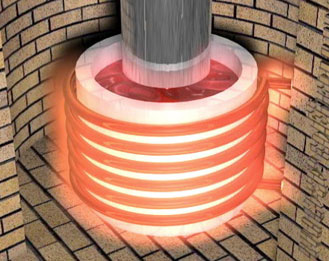
How The Czochralski Process Works
High-purity silicon is melted down in a crucible. A seed crystal mounted on a rod, is dipped into the molten silicon.
The rod is pulled upwards and rotated at the same time.A large, single-crystal, cylindrical ingot is extracted from the melt by precisely controlling the temperature, rate of pulling and speed of rotation.Due to the efficiencies of common wafer specifications, the semiconductor industry has used wafers with standardized dimensions. In the early days, the boules were smaller, only a few inches wide. With advanced technology, high-end device manufacturers use 200 mm and 300 mm diameter wafers. The width is controlled by precise control of the temperature, the speeds of rotation and the speed the seed holder is withdrawn. The crystal ingots from which these wafers are sliced can be up to 2 metres in length, weighing several hundred kilograms. Larger wafers allow improvements in manufacturing efficiency, as more chips can be fabricated on each wafer, so there has been a steady drive to increase silicon wafer sizes. The next step up, 450 mm, is currently scheduled for introduction in 2012. Silicon wafers are typically about 0.2–0.75 mm thick, and can be polished to great flatness for making integrated circuits, or textured for making solar cells.
The process begins when the chamber is heated to approximately 1500 degrees Celsius, melting the silicon. When the silicon is fully melted, a small seed crystal mounted on the end of a rotating shaft is slowly lowered until it just dips below the surface of the molten silicon. The shaft rotates counterclockwise and the crucible rotates clockwise. The rotating rod is then drawn upwards very slowly, allowing a roughly cylindrical boule to be formed. The boule can be from one to two metres, depending on the amount of silicon in the crucible.
The electrical characteristics of the silicon are controlled by adding material like phosphorus or boron to the silicon before it is melted. The added material is called dopant and the process is called doping. This method is also used with semiconductor materials other than silicon, such as gallium arsenide.
Monocrystalline silicon grown by the Czochralski process is the basic material in the production of the large-scale integrated circuit chips used in computers, TVs, cell phones and electronic equipment of all kinds.
Impurity incorporationWhen silicon is grown by the Czochralski method, the melt is contained in a silica (quartz) crucible. During growth, the walls of the crucible dissolve into the melt and Czochralski silicon therefore contains oxygen at a typical concentration of 1018 cm−3. Oxygen impurities can have beneficial effects. Carefully chosen annealing conditions can allow the formation of oxygen precipitates. These have the effect of trapping unwanted transition metal impurities in a process known as gettering. Additionally, oxygen impurities can improve the mechanical strength of silicon wafers by immobilising any dislocations which may be introduced during device processing. It was experimentally shown in the 1990s that the high oxygen concentration is also beneficial for radiation hardness of silicon particle detectors used in harsh radiation environment (such as CERN's LHC/S-LHC projects). Therefore, radiation detectors made of Czochralski- and Magnetic Czochralski-silicon are considered to be promising candidates for many future high-energy physics experiments. It has also been shown that presence of oxygen in silicon increases impurity trapping during post-implantation annealing processes.
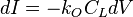
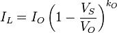
 impurity incorporation from melt :Math Explanation
The impurity concentration in the solid crystal that results from freezing an incremental amount of volume can be obtained from consideration of the segregation coefficient.- kO: Segregation coefficient
- V0: Initial volume
- I0: Number of impurities
- C0: Impurity concentration in the melt
- VL: Volume of the melt
- IL: Number of impurities in the melt
- CL: Concentration of impurities in the melt
- VS: Volume of solid
- CS: Concentration of impurities in the solid