
Transparent conducting films (TCFs) are optically transparent and electrically conductive in thin layers.
TCFs for photovoltaic applications have been fabricated from both inorganic and organic materials. Inorganic films typically are made up of a layer of TCO (transparent conducting oxide), generally in the form of indium tin oxide (ITO), fluorine doped tin oxide (FTO), and doped zinc oxide. Organic films are being developed using carbon nanotube networks and graphene, which can be fabricated to be highly transparent to the infrared light, along with networks of polymers such as poly(3,4-ethylenedioxythiophene) and its derivatives.
 Transparent conducting films act, as a window for light to pass through to the active material beneath (where carrier generation occurs), as an ohmic contact for carrier transport out of the photovoltaic but also as transparent carrier for smd electronics used between laminated glass or light transmissive composites. Transparent materials possess bandgaps with energies corresponding to wavelengths which are shorter than the visible range of 380 nm to 750 nm. As such, photons with energies below the bandgap are not collected by these materials and thus visible light passes through. However, applications such as photovoltaics may require an even broader bandgap to avoid unwanted absorption of the solar spectra.
 Transparent conductive oxides (TCO) are doped metal oxides used in optoelectronic devices such as flat panel displays and photovoltaics (including inorganic devices, organic devices, and dye-sensitized solar cell). Most of these films are fabricated with polycrystalline or amorphous microstructures. On average, these applications use electrode materials that have greater than 80% transmittance of incident light as well as conductivities higher than 103 S/cm for efficient carrier transport. The transmittance of these films, just as in any transparent material, is limited by light scattering at defects and grain boundaries. In general, TCOs for use as thin-film electrodes in solar cells should have a minimum carrier concentration on the order of 1020 cm−3 for low resistivity and a bandgap greater than 380 nm to avoid absorption of light over most of the solar spectra. Mobility in these films is limited by ionized impurity scattering and is on the order of 40 cm2/(V·s). Current transparent conducting oxides used in industry are primarily n-type conductors, meaning their primary conduction is from the flow of electrons. Suitable p-type transparent conducting oxides are still being researched.
To date, the industry standard in TCO is ITO, or tin-doped indium-oxide. This material boasts a low resistivity of ~10−4 Ω·cm and a transmittance of greater than 80%.
However ITO has the drawback of being expensive. Indium, the film’s primary metal, is rare (6000 metric tons worldwide in 2006), and its price fluctuates due to market demand (over $800 per kg in 2006). For this reason, doped binary compounds such as aluminum-doped zinc-oxide (AZO) and indium-doped cadmium-oxide have been proposed as alternative materials. AZO is composed of aluminum and zinc, two common and inexpensive materials, while indium-doped cadmium oxide only uses indium in low concentrations.
Binary compounds of metal oxides without any intentional impurity doping have also been developed for use as TCOs. These systems are typically n-type with a carrier concentration on the order of 1020 cm−3, provided by interstitial metal ions and oxygen vacancies which both act as donors. However, these simple TCOs have not found practical use due to their electrical properties’ high temperature and oxygen partial pressure dependence.
 Doped metal oxides for use as transparent conducting layers in photovoltaic devices are typically grown on a glass substrate. This glass substrate, apart from providing a support that the oxide can grow on, has the additional benefit of blocking most infrared wavelengths greater than 2 µm for most silicates, and converting it to heat in the glass layer. This in turn helps maintain a low temperature of the active region of the solar cell, which degrades in performance as it heats up. TCO films can be deposited on a substrate through various deposition methods, including metal organic chemical vapor deposition (MOCVD), metal organic molecular beam deposition (MOMBD), spray pyrolysis, and pulsed laser deposition (PLD), however conventional fabrication techniques typically involve magnetron sputtering of the film. The sputtering process is very inefficient, with only 30% of the material actually being deposited on the substrate. In the case of ITO this inefficiency is a significant drawback, however work is still underway to increase the recoverable amount of the unused material. Growth typically is performed in a reducing environment to encourage oxygen vacancy formation within the film, which contribute to the carrier concentration (if n-type).
Charge carriers in these oxides arise from three fundamental sources: interstitial metal ion impurities, oxygen vacancies, and doping ions. The first two sources always act as electron donors. Indeed some TCOs are fabricated solely using these two intrinsic sources as carrier generators. When an oxygen vacancy is present in the lattice it acts as a doubly charged electron donor. In ITO, for example, each oxygen vacancy causes the neighboring In3+ ion 5s orbitals to be stabilized from the 5s conduction band by the missing bonds to the oxygen ion, while two electrons are trapped at the site due to charge neutrality effects. This stabilization of the 5s orbitals causes a formation of a donor level for the oxygen ion, determined to be 0.03 eV below the conduction band. Thus these defects act as shallow donors to the bulk crystal. Common notation for this doping is Kröger–Vink notation and is written as:
Dopant ionization within the oxide occurs in the same way as in other semiconductor crystals. Shallow donors near the conduction band (n-type) allow electrons to be thermally excited into the conduction band, while acceptors near the valence band (p-type) allow electrons to jump from the valence band to the acceptor level, populating the valence band with holes. It is important to note that carrier scattering in these oxides arises primarily from ionized impurity scattering. Charged impurity ions and point defects have scattering cross-sections that are much greater than their neutral counterparts. Increasing the scattering decreases the mean-free path of the carriers in the oxide, which leads to poor device performance and a high resistivity. These materials can be modeled reasonably well by the free electron gas theory assuming a parabolic conduction band and doping levels above the Mott Criterion. This criterion states that an insulator such as an oxide can experience a composition-induced transition to a metallic state given a minimum doping concentration nc, determined by:
Transparent conductive polymers can be [are?] used as electrodes on light emitting diodes and photovoltaic devices. They have conductivity below that of transparent conducting oxides but have low absorption of the visible spectrum allowing them to act as a transparent conductor on these devices. However, because transparent conductive polymers do absorb some of the visible spectrum and significant amounts of the mid to near IR, they lower the efficiency of photovoltaic devices.
The transparent conductive polymers can be made into flexible films making them desirable despite their lower conductivity. This makes them useful in the development of flexible electronics where traditional transparent conductors will fail.
 The bandgap of PEDOT can be varied between 1.4 and 2.5 eV by varying the degree of π-overlap along the backbone. This can be done by adding substituents along the chain, which result in steric interactions preventing π-overlap. Substituents can also be electron-accepting or donating which will modify the electronic character and thus modify the bandgap. This allows for the formation of a wide bandgap conductor which is transparent to the visible spectrum.
PEDOT is prepared by mixing EDT monomer with an oxidizing agent such as FeCl3. The oxidizing agent acts as an initiator for polymerization. Research has shown that increasing the ratio of [FeCl3]/[monomer] decreases the solubility of the PEDOT. This is thought to be a result of increased crosslinking in the polymer making it more difficult to dissolve in a solvent.
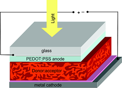 Doping PEDOT with poly(styrene sulfonate) can improve the properties over the unmodified PEDOT. This PEDOT:PSS compound has become the industry leader in transparent conductive polymers. PEDOT:PSS is water soluble making processing easier. PEDOT:PSS has a conductivity ranging from 400 to 600 S/cm while still transmitting ~80% of visible light. Treatment in air at 100 °C for over 1000 hours will result in a minimal change in conductivity.
PEDOT:PSS is prepared by polymerizing EDT monomer in an aqueous solution of PSS using Na2S2O8 as the oxidizing agent. This aqueous solution is then spin coated and dried to make a film.
 DDQ itself has a conductivity of 1.1 S/cm. However, DDQ-doped poly(4,4-dioctylcyclopentadithiophene) also tends to decrease its conductivity in air. DDQ-doped polymer has better stability than the iodine-doped polymer, but the stability is still below that of PEDOT. In summary, poly(4,4-dioctylcyclopentadithiophene) has inferior properties relative to PEDOT and PEDOT:PSS, which need to be improved for realistic applications.
Poly(4,4-dioctylcyclopentadithiophene) is solution polymerized by combining monomer with iron(III) chloride. Once the polymerization is complete the doping is done by exposing the polymer to iodine vapor or DDQ solution.
Carbon nanotubes (CNTs) have attracted much attention because of their materials properties, including a high elastic modulus (~1–2 TPa), a high tensile strength (~13–53 GPa), and a high conductivity (metallic tubes can theoretically carry an electrical current density of 4×10⁹ A/cm2, which is ~1000 times higher than for other metals such as copper). CNT thin films have been used as transparent electrodes in TCFs because of these good electronic properties.
Properties Of Indium Tin Oxide
ITO is a heavily-doped n-type semiconductor with a large bandgap. Because of the bandgap, it is mostly transparent in the visible part of the spectrum. In the ultraviolet, it is opaque because of band-to-band absorption (a UV photon can excite an electron from the valence band to the conduction band). In the near infrared, it also opaque, because of free carrier absorption (an infrared photon can excite an electron from near the bottom of the conduction band to higher within the conduction band).
TCFs for photovoltaic applications have been fabricated from both inorganic and organic materials. Inorganic films typically are made up of a layer of TCO (transparent conducting oxide), generally in the form of indium tin oxide (ITO), fluorine doped tin oxide (FTO), and doped zinc oxide. Organic films are being developed using carbon nanotube networks and graphene, which can be fabricated to be highly transparent to the infrared light, along with networks of polymers such as poly(3,4-ethylenedioxythiophene) and its derivatives.
Transparent conducting films act, as a window for light to pass through to the active material beneath (where carrier generation occurs), as an ohmic contact for carrier transport out of the photovoltaic but also as transparent carrier for smd electronics used between laminated glass or light transmissive composites. Transparent materials possess bandgaps with energies corresponding to wavelengths which are shorter than the visible range of 380 nm to 750 nm. As such, photons with energies below the bandgap are not collected by these materials and thus visible light passes through. However, applications such as photovoltaics may require an even broader bandgap to avoid unwanted absorption of the solar spectra.Transparent conductive oxides (TCO) are doped metal oxides used in optoelectronic devices such as flat panel displays and photovoltaics (including inorganic devices, organic devices, and dye-sensitized solar cell). Most of these films are fabricated with polycrystalline or amorphous microstructures. On average, these applications use electrode materials that have greater than 80% transmittance of incident light as well as conductivities higher than 103 S/cm for efficient carrier transport. The transmittance of these films, just as in any transparent material, is limited by light scattering at defects and grain boundaries. In general, TCOs for use as thin-film electrodes in solar cells should have a minimum carrier concentration on the order of 1020 cm−3 for low resistivity and a bandgap greater than 380 nm to avoid absorption of light over most of the solar spectra. Mobility in these films is limited by ionized impurity scattering and is on the order of 40 cm2/(V·s). Current transparent conducting oxides used in industry are primarily n-type conductors, meaning their primary conduction is from the flow of electrons. Suitable p-type transparent conducting oxides are still being researched.To date, the industry standard in TCO is ITO, or tin-doped indium-oxide. This material boasts a low resistivity of ~10−4 Ω·cm and a transmittance of greater than 80%.
However ITO has the drawback of being expensive. Indium, the film’s primary metal, is rare (6000 metric tons worldwide in 2006), and its price fluctuates due to market demand (over $800 per kg in 2006). For this reason, doped binary compounds such as aluminum-doped zinc-oxide (AZO) and indium-doped cadmium-oxide have been proposed as alternative materials. AZO is composed of aluminum and zinc, two common and inexpensive materials, while indium-doped cadmium oxide only uses indium in low concentrations.
Binary compounds of metal oxides without any intentional impurity doping have also been developed for use as TCOs. These systems are typically n-type with a carrier concentration on the order of 1020 cm−3, provided by interstitial metal ions and oxygen vacancies which both act as donors. However, these simple TCOs have not found practical use due to their electrical properties’ high temperature and oxygen partial pressure dependence.
Doped metal oxides for use as transparent conducting layers in photovoltaic devices are typically grown on a glass substrate. This glass substrate, apart from providing a support that the oxide can grow on, has the additional benefit of blocking most infrared wavelengths greater than 2 µm for most silicates, and converting it to heat in the glass layer. This in turn helps maintain a low temperature of the active region of the solar cell, which degrades in performance as it heats up. TCO films can be deposited on a substrate through various deposition methods, including metal organic chemical vapor deposition (MOCVD), metal organic molecular beam deposition (MOMBD), spray pyrolysis, and pulsed laser deposition (PLD), however conventional fabrication techniques typically involve magnetron sputtering of the film. The sputtering process is very inefficient, with only 30% of the material actually being deposited on the substrate. In the case of ITO this inefficiency is a significant drawback, however work is still underway to increase the recoverable amount of the unused material. Growth typically is performed in a reducing environment to encourage oxygen vacancy formation within the film, which contribute to the carrier concentration (if n-type). Charge carriers in these oxides arise from three fundamental sources: interstitial metal ion impurities, oxygen vacancies, and doping ions. The first two sources always act as electron donors. Indeed some TCOs are fabricated solely using these two intrinsic sources as carrier generators. When an oxygen vacancy is present in the lattice it acts as a doubly charged electron donor. In ITO, for example, each oxygen vacancy causes the neighboring In3+ ion 5s orbitals to be stabilized from the 5s conduction band by the missing bonds to the oxygen ion, while two electrons are trapped at the site due to charge neutrality effects. This stabilization of the 5s orbitals causes a formation of a donor level for the oxygen ion, determined to be 0.03 eV below the conduction band. Thus these defects act as shallow donors to the bulk crystal. Common notation for this doping is Kröger–Vink notation and is written as:


Dopant ionization within the oxide occurs in the same way as in other semiconductor crystals. Shallow donors near the conduction band (n-type) allow electrons to be thermally excited into the conduction band, while acceptors near the valence band (p-type) allow electrons to jump from the valence band to the acceptor level, populating the valence band with holes. It is important to note that carrier scattering in these oxides arises primarily from ionized impurity scattering. Charged impurity ions and point defects have scattering cross-sections that are much greater than their neutral counterparts. Increasing the scattering decreases the mean-free path of the carriers in the oxide, which leads to poor device performance and a high resistivity. These materials can be modeled reasonably well by the free electron gas theory assuming a parabolic conduction band and doping levels above the Mott Criterion. This criterion states that an insulator such as an oxide can experience a composition-induced transition to a metallic state given a minimum doping concentration nc, determined by:
Conducting polymers (Transparent)
 Conductive polymers were reported in the mid the 20th century as derivatives of polyaniline. Research continued on such polymers in the 1960s and 70s and continued into the turn of the 21st century. Most conductive polymers are derivatives of polyacetylene, polyaniline, polypyrrole or polythiophenes. These polymers have conjugated double bonds which allow for conduction. By manipulating the band structure, polythiophenes have been modified to achieve a HOMO-LUMO separation (bandgap) that is large enough to make them transparent to visible light.
Transparent conductive polymers can be [are?] used as electrodes on light emitting diodes and photovoltaic devices. They have conductivity below that of transparent conducting oxides but have low absorption of the visible spectrum allowing them to act as a transparent conductor on these devices. However, because transparent conductive polymers do absorb some of the visible spectrum and significant amounts of the mid to near IR, they lower the efficiency of photovoltaic devices.The transparent conductive polymers can be made into flexible films making them desirable despite their lower conductivity. This makes them useful in the development of flexible electronics where traditional transparent conductors will fail.
Poly(3,4-ethylenedioxythiophene) (PEDOT)
Poly(3,4-ethylenedioxythiophene) (PEDOT) has conductivity of up to around 1,000 S/cm. Thin oxidized PEDOT films have approx. 10% or less absorption in the visible spectrum and excellent stability. However, PEDOT is insoluble in water making processing more difficult and costly.The bandgap of PEDOT can be varied between 1.4 and 2.5 eV by varying the degree of π-overlap along the backbone. This can be done by adding substituents along the chain, which result in steric interactions preventing π-overlap. Substituents can also be electron-accepting or donating which will modify the electronic character and thus modify the bandgap. This allows for the formation of a wide bandgap conductor which is transparent to the visible spectrum.PEDOT is prepared by mixing EDT monomer with an oxidizing agent such as FeCl3. The oxidizing agent acts as an initiator for polymerization. Research has shown that increasing the ratio of [FeCl3]/[monomer] decreases the solubility of the PEDOT. This is thought to be a result of increased crosslinking in the polymer making it more difficult to dissolve in a solvent.
Poly(3,4-ethylenedioxythiophene) PEDOT: poly(styrene sulfonate) PSS
Doping PEDOT with poly(styrene sulfonate) can improve the properties over the unmodified PEDOT. This PEDOT:PSS compound has become the industry leader in transparent conductive polymers. PEDOT:PSS is water soluble making processing easier. PEDOT:PSS has a conductivity ranging from 400 to 600 S/cm while still transmitting ~80% of visible light. Treatment in air at 100 °C for over 1000 hours will result in a minimal change in conductivity.PEDOT:PSS is prepared by polymerizing EDT monomer in an aqueous solution of PSS using Na2S2O8 as the oxidizing agent. This aqueous solution is then spin coated and dried to make a film.
Poly(4,4-dioctylcyclopentadithiophene)
Poly(4,4-dioctylcyclopentadithiophene) can be doped with iodine or 2,3-dichloro-5,6-dicyano-1,4-benzoquinone (DDQ) to form a transparent conductor. The doped polymer has low absorption of the visible spectrum with an absorption band centered around 1050 nm. When doped with iodine, a conductivity of 0.35 S/cm can be achieved. However, the iodine has a tendency to diffuse out in air, making the iodine-doped poly(4,4-dioctylcyclopentadithiophene) unstable.DDQ itself has a conductivity of 1.1 S/cm. However, DDQ-doped poly(4,4-dioctylcyclopentadithiophene) also tends to decrease its conductivity in air. DDQ-doped polymer has better stability than the iodine-doped polymer, but the stability is still below that of PEDOT. In summary, poly(4,4-dioctylcyclopentadithiophene) has inferior properties relative to PEDOT and PEDOT:PSS, which need to be improved for realistic applications.Poly(4,4-dioctylcyclopentadithiophene) is solution polymerized by combining monomer with iron(III) chloride. Once the polymerization is complete the doping is done by exposing the polymer to iodine vapor or DDQ solution.
Advantages Of TCF
Transparent conductors are fragile and tend to break down due to fatigue. The most commonly used TCF is Indium-Tin-Oxide (ITO) because of its good electrical properties and ease of fabrication. However, these thin films are usually fragile and such problems as lattice mismatch and stress-strain constraints lead to restrictions in possible uses for TCFs. ITO has been shown to degrade with time when subject to mechanical stresses. Recent increases in cost are also forcing many to look to carbon nanotube films as a potential alternative.Carbon nanotubes (CNTs) have attracted much attention because of their materials properties, including a high elastic modulus (~1–2 TPa), a high tensile strength (~13–53 GPa), and a high conductivity (metallic tubes can theoretically carry an electrical current density of 4×10⁹ A/cm2, which is ~1000 times higher than for other metals such as copper). CNT thin films have been used as transparent electrodes in TCFs because of these good electronic properties.
Properties Of Indium Tin Oxide
ITO is a heavily-doped n-type semiconductor with a large bandgap. Because of the bandgap, it is mostly transparent in the visible part of the spectrum. In the ultraviolet, it is opaque because of band-to-band absorption (a UV photon can excite an electron from the valence band to the conduction band). In the near infrared, it also opaque, because of free carrier absorption (an infrared photon can excite an electron from near the bottom of the conduction band to higher within the conduction band).


