
A solid-state laser is a laser that uses a gain medium that is a solid, rather than a liquid such as in dye lasers or a gas as in gas lasers. Semiconductor-based lasers are also in the solid state, but are generally considered as a separate class from solid-state lasers (see Laser diode).
 Generally, the active medium of a solid-state laser consists of a glass or crystalline host material to which is added a dopant such as neodymium, chromium, erbium, or other ions. Many of the common dopants are rare earth elements, because the excited states of such ions are not strongly coupled with thermal vibrations of the crystalline lattice (phonons), and the lasing threshold can be reached at relatively low brightness of pump.
There are many hundreds of solid-state media in which laser action has been achieved, but relatively few types are in widespread use. Of these, probably the most common is neodymium-doped YAG. Neodymium-doped glass (Nd:glass) and ytterbium-doped glasses and ceramics are used in extremely high power (terawatt scale), high energy (megajoules) multiple beam systems for inertial confinement fusion.
The first material used for lasing was ruby. Ruby lasers are still used for some applications, but are not common due to their low efficiency. Er:YAG lasers lase in the mid-infrared.
Some solid-state lasers can also be tunable using several intracavity techniques which employ etalons, prisms, and gratings, or a combination of these. Titanium-doped sapphire is widely used for its broad tuning range, 660–986 nm. Alexandrite lasers are tunable from 700 to 820 nm and offer higher pulse energies then Ti-Sapphire due to their longer storage time and high damage threshold.
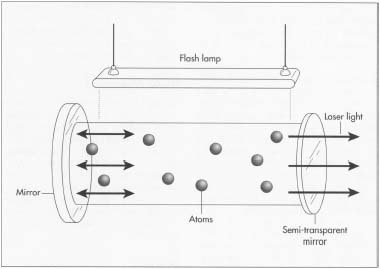
Solid state lasing media are typically optically pumped, using either a flashlamp or arc lamp, or by laser diodes. Diode-pumped solid-state lasers tend to be much more efficient, and have become much more common as the cost of high power semiconductor lasers has decreased.
Lets Take a Look at Cadmium Sulfide (A good example of Solid state Laser)
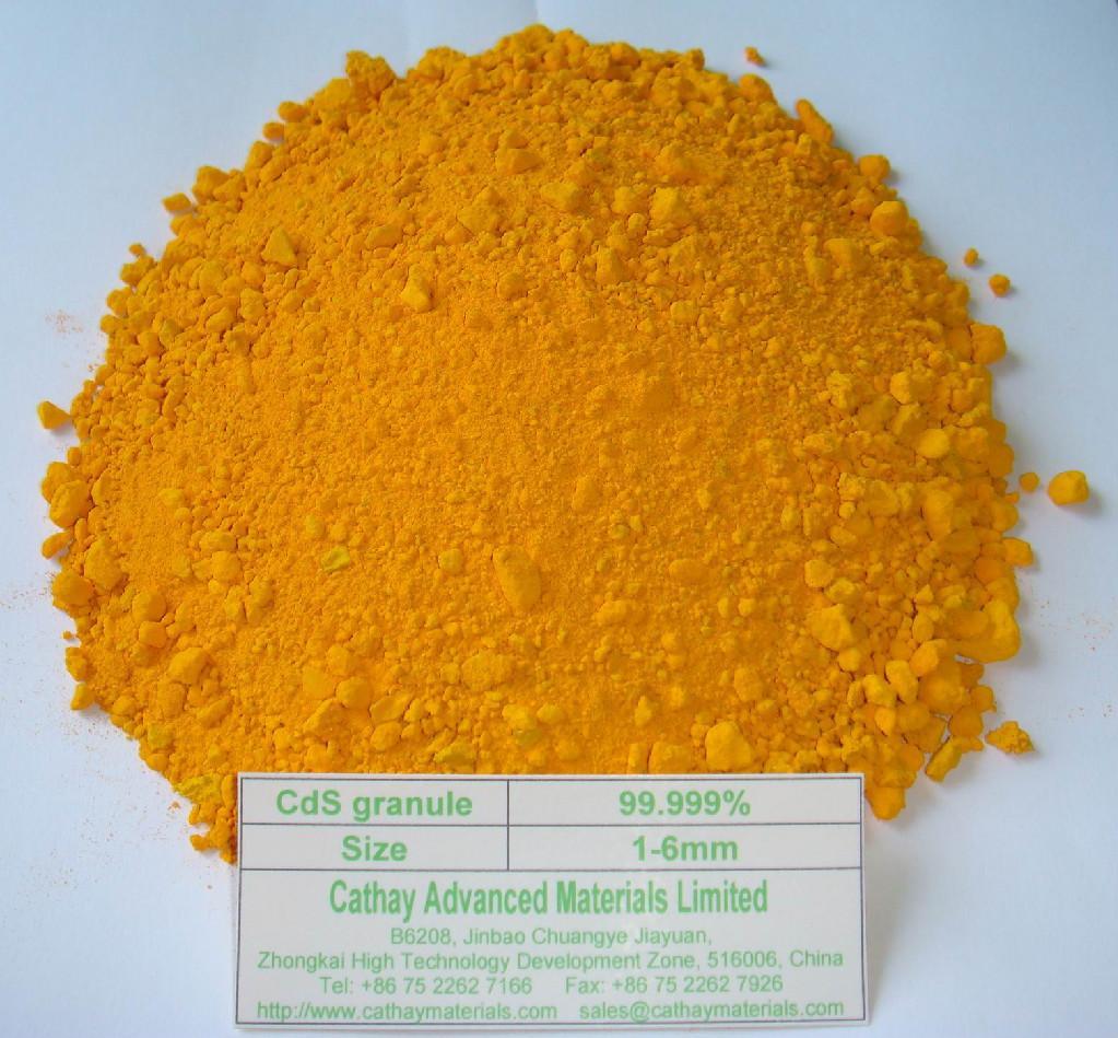
Cadmium sulfide is the inorganic compound with the formula CdS. Cadmium sulfide is a yellow solid. It occurs in nature with two different crystal structures as the rare minerals greenockite and hawleyite, but is more prevalent as an impurity substituent in the similarly structured zinc ores sphalerite and wurtzite, which are the major economic sources of cadmium. As a compound that is easy to isolate and purify, it is the principal source of cadmium for all commercial applications.
Cadmium sulfide can be prepared by the precipitation from soluble cadmium(II) salts with sulfide ion and this has been used in the past for gravimetric analysis and qualitative inorganic analysis.
Pigment production usually involves the precipitation of CdS, the washing of the precipitate to remove soluble cadmium salts followed by calcination (roasting) to convert it to the hexagonal form followed by milling to produce a powder. When cadmium sulfide selenides are required the CdSe is co-precipitated with CdS and the cadmium sulfoselenide is created during the calcination step.
Industrially the production of thin films of CdS, required in e.g. photoresistors and chemical bath deposition (CBD), has been investigated using the hydrolysis of thiourea as the source of sulfide anions and an ammonium salt /ammonia buffer solution to control pH:
The preparative route and the subsequent treatment of the product, affects the polymorphic form that is produced. It has been asserted that chemical precipitation methods result in the cubic zinc blende form.
 Thin films of CdS are components in some photoresistors and solar cells. Various methods have been used to deposit these thin films, for example (note: there is a large body of research in this area and only representative references are given):
Cadmium sulfide has, like zinc sulfide, two crystal forms; the more stable hexagonal wurtzite structure (found in the mineral Greenockite) and the cubic zinc blende structure (found in the mineral Hawleyite). In both of these forms the cadmium and sulfur atoms are four coordinate. There is also a high pressure form with the NaCl rock salt structure.
Cadmium sulfide is a direct band gap semiconductor (gap 2.42 eV). The magnitude of its band gap means that it appears coloured.
As well as this obvious property others properties result:
Generally, the active medium of a solid-state laser consists of a glass or crystalline host material to which is added a dopant such as neodymium, chromium, erbium, or other ions. Many of the common dopants are rare earth elements, because the excited states of such ions are not strongly coupled with thermal vibrations of the crystalline lattice (phonons), and the lasing threshold can be reached at relatively low brightness of pump.There are many hundreds of solid-state media in which laser action has been achieved, but relatively few types are in widespread use. Of these, probably the most common is neodymium-doped YAG. Neodymium-doped glass (Nd:glass) and ytterbium-doped glasses and ceramics are used in extremely high power (terawatt scale), high energy (megajoules) multiple beam systems for inertial confinement fusion.
The first material used for lasing was ruby. Ruby lasers are still used for some applications, but are not common due to their low efficiency. Er:YAG lasers lase in the mid-infrared.
Some solid-state lasers can also be tunable using several intracavity techniques which employ etalons, prisms, and gratings, or a combination of these. Titanium-doped sapphire is widely used for its broad tuning range, 660–986 nm. Alexandrite lasers are tunable from 700 to 820 nm and offer higher pulse energies then Ti-Sapphire due to their longer storage time and high damage threshold.
Solid state lasing media are typically optically pumped, using either a flashlamp or arc lamp, or by laser diodes. Diode-pumped solid-state lasers tend to be much more efficient, and have become much more common as the cost of high power semiconductor lasers has decreased.
Lets Take a Look at Cadmium Sulfide (A good example of Solid state Laser)
Cadmium sulfide is the inorganic compound with the formula CdS. Cadmium sulfide is a yellow solid. It occurs in nature with two different crystal structures as the rare minerals greenockite and hawleyite, but is more prevalent as an impurity substituent in the similarly structured zinc ores sphalerite and wurtzite, which are the major economic sources of cadmium. As a compound that is easy to isolate and purify, it is the principal source of cadmium for all commercial applications.
Cadmium sulfide can be prepared by the precipitation from soluble cadmium(II) salts with sulfide ion and this has been used in the past for gravimetric analysis and qualitative inorganic analysis.
Pigment production usually involves the precipitation of CdS, the washing of the precipitate to remove soluble cadmium salts followed by calcination (roasting) to convert it to the hexagonal form followed by milling to produce a powder. When cadmium sulfide selenides are required the CdSe is co-precipitated with CdS and the cadmium sulfoselenide is created during the calcination step.
Industrially the production of thin films of CdS, required in e.g. photoresistors and chemical bath deposition (CBD), has been investigated using the hydrolysis of thiourea as the source of sulfide anions and an ammonium salt /ammonia buffer solution to control pH:
- Cd2+ + 4 NH3 → [Cd(NH3)4]2+
- (NH2)2CS + OH− → SH− + H2O + H2CN2
- SH− + Cd2+ → CdS + H+
The preparative route and the subsequent treatment of the product, affects the polymorphic form that is produced. It has been asserted that chemical precipitation methods result in the cubic zinc blende form.
Routes to thin films of CdS
- Chemical bath deposition, CBD
- Sol gel techniques
- MOCVD
- Sputtering
- Electrochemical deposition[11]
- Spraying with precursor cadmium salt, sulfur compound and dopant
- Screen printing using a slurry containing dispersed CdS
 Structure and physical properties
Cadmium sulfide has, like zinc sulfide, two crystal forms; the more stable hexagonal wurtzite structure (found in the mineral Greenockite) and the cubic zinc blende structure (found in the mineral Hawleyite). In both of these forms the cadmium and sulfur atoms are four coordinate. There is also a high pressure form with the NaCl rock salt structure.Cadmium sulfide is a direct band gap semiconductor (gap 2.42 eV). The magnitude of its band gap means that it appears coloured.
As well as this obvious property others properties result:
- the conductivity increases when irradiated with light(leading to uses as a photoresistor)
- when combined with a p-type semiconductor it forms the core component of a photovoltaic (solar) cell and a CdS/Cu2S solar cell was one of the first efficient cells to be reported (1954)
- when doped with for example Cu+ ("activator") and Al3+ ("coactivator") CdS luminesces under electron beam excitation (cathodoluminescence) and is used as phosphor
- both polymorphs are piezoelectric and the hexagonal is also pyroelectric
- electroluminescence
- CdS crystal can act as a solid state laser

